3. Power Amplifier
The power amplifier provides the amplification required to produce audible sound on the loudspeakers. It also serves as a filter, removing unwanted frequency components.
Frequency Dependent Amplification with an Op-amp
As you may recall from Linear Circuits, an op-amp circuit with a purely resistive coupling network has frequency-independent amplification. If at least one frequency-dependent impedance (such as a capacitor) is introduced, the amplification becomes frequency dependent. As a result, the gain is no longer the same for all frequencies.
In the following section, we examine simple first-order filter circuits. These are obtained by replacing one of the impedances in the coupling network with a resistor-capacitor combination. The remaining impedances are resistors. Depending on the configuration, the circuit exhibits either high-pass or low-pass behavior.
Assignments
1. Inverting Amplifier with a First-order Low-pass Filter

Figure 1:An inverting amplifier with a first-order low-pass filter.
Assignments:
Derive the transfer function .
Show that the transfer function has the form
Express and in terms of , , and .
Show that the power transfer equals for .
Sketch as a function of frequency.
Repeat the sketch using a logarithmic frequency scale. Plot on the x-axis and (in dB) on the y-axis.
Show that at is equal to -3 dB relative to its value at . This is therefore also called the -3 dB frequency, denoted .
Show that for , decreases by a factor of ~4 (6 dB) for each doubling of frequency. For this reason, is also called the cut-off frequency: below the transfer is flat, above the transfer decreases.
2. Inverting Amplifier with a First-order High-pass Filter

Figure 2:An inverting op-amp circuit with a first-order high-pass filter.
Assignments:
Derive the transfer function .
Show that it has the form
Express and in terms of , , and .
Show that for .
Sketch as a function of frequency.
Repeat the sketch on a logarithmic frequency scale, plotting .
Show that at is equal to -3 dB relative to the value for . Thus, is also called the -3 dB frequency .
Show that for , decreases by a factor of ~4 (6 dB) for each halving of the frequency.
3. Non-inverting Amplifier with a First-order Low-pass Filter

Figure 3:A non-inverting op-amp circuit with a first-order low-pass filter. This circuit is often used to limit the amplifier input bandwidth, for example above 20 kHz.
Assignments:
Derive .
Show that
Express and in terms of , , , and .
Show that at .
Sketch vs. frequency.
Repeat the sketch on a logarithmic frequency scale, plotting .
Show that at is -3 dB relative to .
Show that for , decreases by a factor of ~4 (6 dB) for each doubling of frequency.
4. Non-inverting Amplifier with a First-order High-pass Filter (1)

Figure 4:A non-inverting op-amp with a first-order high-pass filter. Commonly used to block very low frequencies ( Hz) and DC offsets, which could otherwise damage speakers.
Assignments:
Derive the transfer function .
Show that the transfer function is of the following form:
and express , , and in terms of the component values , , , , and .
Show that and that the power transfer if . This assumption holds for the following assignments.
Show that for , . Furthermore, show that for (this is for ), .
Sketch the power transfer function as a function of the frequency.
Repeat the sketch on a logarithmic frequency scale, plotting .
Show that the value of for the frequency is -3 dB relative to the value for . is therefore sometimes referred to as the -3dB frequency ().
Show that for frequencies , the value of decreases by a factor of ~4 (6 dB) for each halving of the frequency.
5. Non-inverting Amplifier with a First-order High-pass Filter (2)

Figure 5:Another non-inverting op-amp with a first-order high-pass filter. This version completely blocks DC and subsonic signals.
Assignments:
Derive the transfer function .
Show that the transfer function is of the following form:
and express and in terms of the component values , , , and .
Show that the power transfer for .
Sketch the power transfer function as a function of the frequency.
Repeat the sketch on a logarithmic frequency scale, plotting .
Show that the value of for the frequency is -3 dB relative to the value for . is therefore sometimes referred to as the -3dB frequency ().
Show that for frequencies , the value of decreases by a factor of ~4 (6 dB) for each halving of the frequency.
Power Amplifier Circuit

Figure 6:Circuit diagram of the power amplifier that will be used for the audio system.
The power amplifier used in this project is shown in Figure 6. It is based on the LM3886 op-amp. You are provided with a universal amplifier PCB that allows building the schematic shown in Figure 7 and Figure 8.
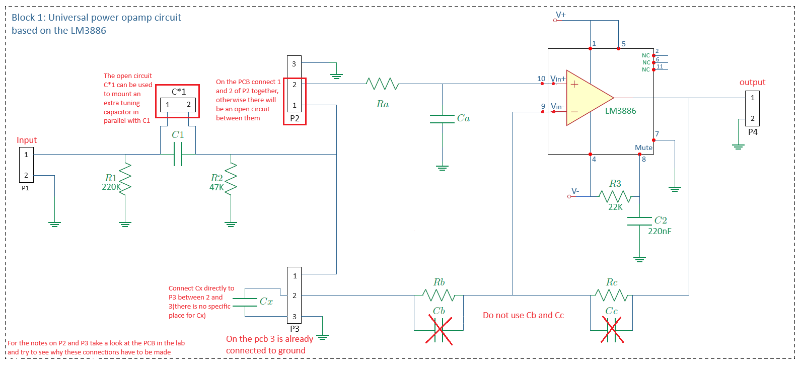
Figure 7:Universal amplifier circuit.
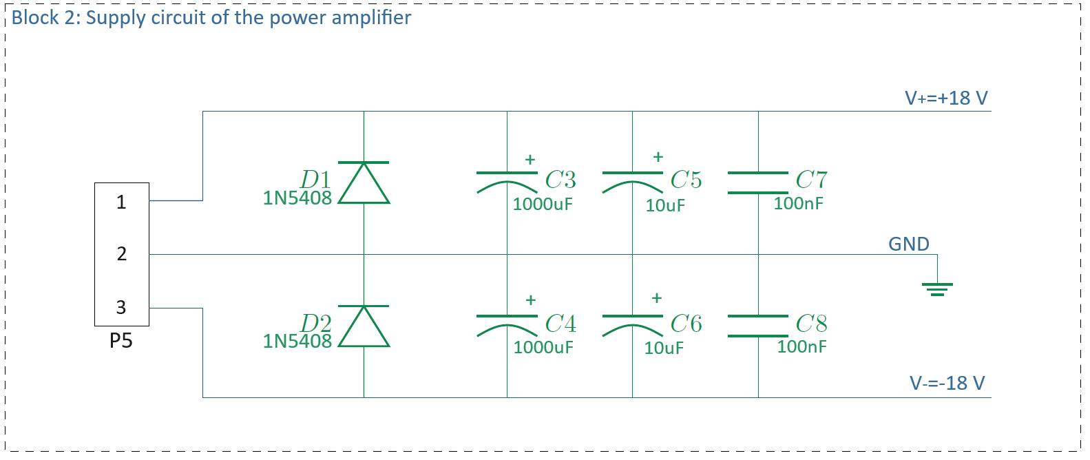
Figure 8:Supply circuit of the audio amplifier.
The circuit consists of:
The universal amplifier circuit.
The power supply circuit.
The universal amplifier can be configured as inverting or non-inverting, with optional filters depending on which components (, , , , , ) are placed or omitted. Connections are made via jumpers at and .
The input connector is , and the output connector is .
The supply circuit includes diodes (, ) for reverse polarity protection and capacitor combinations (–) for filtering. Electrolytic capacitors are paired with ceramics to ensure effective high-frequency filtering.
Building the Circuit
The double-sided PCB is shown in Figure 9 and Figure 10:

Figure 9:Component side of the power amplifier PCB, showing the silk screen.

Figure 10:Silk screen including the traces.
What is a silk screen?
A silk screen (also called silkscreen or solder mask overlay) is a printed layer on a PCB that shows component labels, reference designators (like R1, C1, IC1), component outlines, and other helpful text or symbols. It helps identify where components should be placed and provides important information for assembly and troubleshooting. The silk screen is typically white or yellow text/graphics printed on top of the solder mask.
Connector usage:
, , : green screw connectors.
, : pin headers. Note that the square markers identify Pin 1. That implies that Pin 3 of both of these headers is connected to ground.
Selectable components: slide-headers, often with components soldered to short pin-headers.
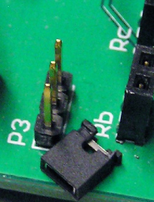
Figure 11:3-pin pin header and jumper cap
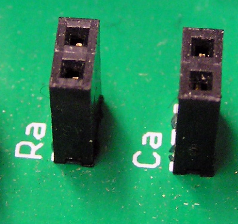
Figure 12:Socket header
Figure 13:Component soldered to a pin header
Assignment
Step 1: Design
Determine the function of each component in the amplifier circuit and select component values such that the amplifier meets the following requirements:
The amplifier circuit has a non-inverting configuration.
The voltage gain in the passband equals 25.
The passband of the amplifier is 20 Hz-40 kHz (-3 dB bandwidth). This means that the signal components with frequencies 𝑓 < 20 Hz and 𝑓 > 40 kHz will be suppressed, relative to the signal components with frequencies of 20 Hz < 𝑓 < 40 kHz.
The DC gain of the amplifier must be 1. This prevents and amplified version of the input offset voltage to be present at the output.
What is input offset voltage?
In a perfect op-amp, equal voltages at both inputs should produce zero output. However, manufacturing tolerances create component mismatches that result in a small DC offset voltage (typically a few millivolts) appearing between the inputs. This offset gets amplified by the circuit’s DC gain, potentially creating a significant DC error at the output.
In audio applications, this DC component can:
Damage speakers if the offset is large enough
Reduce the available dynamic range
Cause audible pops or clicks when the amplifier is turned on/off
That’s why requirement 4 specifies that the DC gain must be 1 - this prevents the amplification of any input offset voltage, keeping the DC output close to zero even if there’s a small offset present at the input.
Convert your theoretical component values into values that are available according to what components are available (see E-series). Make sure that you adjust in the right direction so that the requirements are still met (with a margin).
Step 2: Simulate
You must simulate the circuit in LTspice to confirm it meets requirements 2 and 3 (see Step 1: Design) before building it.
It suffices to use a generic/universal LTSpice op amp model, the UniversalOpAmp2 model as is readily available in LTSpice is recommended. While an actual LM3866 op amp model does exist, there is no benefit for our purposes.
If any or more of the requirements are not met, go into problem solving mode (Problem Solving in Engineering). If the gain at the low frequency crossover point (20 Hz) is inaccurate and/or the roll-off is not 6 dB/octave, suspect that the DC bias block (with is interfering with the high pass filter formed by and .
Step 3: Build
Observe component polarity (diodes, electrolytic capacitors).
Check resistor values (color code and multimeter).
Ensure clean solder joints.
Mount and solder all components except for the heat sink, op amp and both 1000 F capacitors.
will be used to connect . can be soldered in directly, no need for a pin header.
Pin 1 and Pin 2 of can be connected with either a wire or with a header and a jumper cap over it.
For easy configurablity, you might consider using components soldered to pin headers (Figure 13) and insert them in a socket header (Figure 12).
Attach op-amp to heat sink: Mount the op-amp to the heat sink using an M3 screw before soldering. The heat sink has two horizontal grooves for mounting the op amp, use the lower one. Take care that the op amp is centered in the middle of the heat sink. Verify there is no gap between the back of the op-amp and the heat sink by checking from the side that no light can pass through. If there is a gap, the heat sink will be unable to cool the chip.
Solder op-amp to PCB: Place the op-amp on the PCB with the leads protruding through the holes, then solder it in place.
Mount heat sink to PCB: Attach the heat sink to the PCB using four M3 screws. You may need to apply gentle pressure to fit it properly. If the PCB holes don’t match the mounting positions of the heat sink, choose one of these options:
Option A: Leave the heat sink floating, relying on its attachment to the op-amp for mechanical stability.
Option B: Loosen the op-amp mounting screw, secure the heat sink to the PCB first, then remount the op-amp with a thin layer of thermal paste between the op-amp’s metal surface and the heat sink.
Finally solder the 1000 F capacitors.
See the next section for Visual Inspection.
Why a heat sink?
A heat sink is essential for the LM3886 power amplifier because it dissipates heat generated during operation. Power amplifiers convert some of the input power into heat rather than useful output power - this is especially significant when driving loads or operating at high power levels.
Without adequate cooling, the chip temperature can rise to dangerous levels, causing:
Activation of built-in thermal protection (reducing output power)
Permanent damage to the op-amp
Unstable operation or complete failure
The heat sink provides a large surface area to transfer heat away from the chip to the surrounding air, keeping the operating temperature within safe limits and ensuring reliable performance.
What is thermal paste?
Thermal paste (also called thermal compound or thermal grease) is a thermally conductive material applied between a heat-generating component (like the LM3886 op-amp) and its heat sink. It fills microscopic air gaps and surface irregularities to improve heat transfer. However, if the op-amp and heat sink surfaces are flat and make good contact, thermal paste may not be necessary for this application. If you did not succeed in making a good connection, thermal paste can be solution.
See Figure 14 for a completed build.
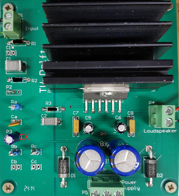
Figure 14:Example PCB of a completed power amplifier.
Step 4: Inspect
Check your build for visual defects.
Use a magnifying glass or your phone camera with zoom if needed to inspect closely. Good lighting is essential for effective visual inspection.
Solder joints:
All joints should be shiny and smooth (not dull or grainy)
No cold solder joints (insufficient solder or poor contact)
No solder bridges between adjacent pins or traces
No excessive solder that could create shorts
Component placement:
All components are in their correct locations according to the schematic and PCB layout
Polarized components (electrolytic capacitors, diodes, op-amp) are oriented correctly
No components are missing
Component integrity:
No damaged or cracked components
No bent or broken leads
Heat sink is properly mounted with no gaps
PCB condition:
No damaged traces or pads
No solder splashes or debris on the board
Connections:
All required connections are made
No loose wires or poorly secured connectors
Power supply connections are correct (check polarity)
If you find any issues, correct them before proceeding to testing.
See Problem Solving in Engineering.
Step 5: Test
Testing involves checking the actual circuits complies with the requirements through measurements, and determining the actual specifications of the circuit.
Before actual testing, you need to perform a controlled power up of the circuit. Such a step is to prevent the occurrence of cascading damage from high currents if there accidentally is a short circuit that has not be discovered during visual inspection.
Controlled Power Up
Use the digital power supply
Set the voltage to 15 V and the maximum current to 250 mA. 15 V means that there is 7.5 V from + to GND and from GND to -.
Double check the connections from power supply to the PCB: + to +, - to - and GND to GND.
Make sure that there is no load connected to the amplifier.
Power up the circuit. If the supply voltage drops and/or the current draw reaches 250 mA, there is a problem, probably a short circuit somewhere. Embark on problem solving, see Problem Solving in Engineering.
If all goes well, you can connect the analog power supply at 2 x 15 V (30 V total), connect a signal generator to the input of the amplifier. 1000 Hz is a good frequency and 0.5 V is a good amplitude. Then, connect an osciloscope to the output, and check if you can see an amplified signal on the scope. If yes: SUCCESS.
If you have reached this point, the next activity is actual checking if the requirements are met.
Checking Requirements
Requirement 1 need not be checked explicitly, it is fulfilled by construction.
Requirement 2 can be checked using a signal generator and an oscilloscope, at a frequency far enough from the cross-over frequencies such as 1000 Hz. You can visualize both the input and the output signal on the oscilloscope and measure of both. The ratio should be (approximately) equal to your calculated gain given the values of the resistors in your feedback network. (Note that you should also see that the output is the inverse of the input, as per Requirement 1.)
Requirement 3 should be checked in the same way, but then check the expected gain at both crossover frequencies. Also check the roll-off, it should be 6 dB per octave / 20 dB per decade. It is nice if you measure the gain at multiple frequencies so that you could actually prepare a frequency-gain plot for in the final report.
Requirement 4 can be checked by leaving the input open (disconnect the signal generator) since resistors and will then provide a path to ground for the input of the op-amp. Then, measure the DC voltage at the output. It should be no more than the maximum value of the offset input voltage as listed in the LM3866 data sheet.
What is a data sheet? Where to find it?
A data sheet is a technical document provided by component manufacturers that contains detailed specifications, characteristics, and operating parameters for electronic components like integrated circuits, transistors, and other devices.
For the LM3886 op-amp used in this project, the data sheet includes:
Maximum offset input voltage specifications
Operating voltage ranges
Current consumption
Thermal characteristics
Pin configurations
Application circuits
Performance graphs
and much more
Where to find data sheets:
Manufacturer websites: Texas Instruments (TI) is the original manufacturer of the LM3886
Distributor websites: Digi-Key, Mouser, RS Components, etc.
Search engines: Simply search “LM3886 datasheet PDF”
Component databases: Sites like AllDataSheet.com or DataSheetCatalog
.org
Always use official manufacturer data sheets when possible, as they contain the most accurate and up-to-date information for your design and testing requirements. The order given in the list of search locations above is typically a good search order.
If any or more of the requirements are not met, go into problem solving mode (Problem Solving in Engineering). If the gain at the low frequency crossover point (20 Hz) is inaccurate and/or the roll-off is not 6 dB/octave, suspect that the DC bias block (with is interfering with the high pass filter formed by and .
If all is well: you are ready for final integration with the power supply and the filters.