2. Power Supply
Introduction
The power supply converts the 230 Vrms grid voltage into a DC voltage. This voltage is then used by the opamps in the power amplifier, and eventually the bass extension, to increase the available power of the signal.
This module guides you through the steps of designing a power supply from scratch.
Theory: The Power Supply Circuit
The power supply circuit that you must use in the IP-1 project is shown in Figure 1. The AC input voltage is first scaled down by a transformer, then rectified by a diode circuit, and then filtered by an RC-circuit. Note that many other AC-to-DC conversion circuits exist, but their design and the differences between them is the topic of a future course, and outside the scope of IP-1.

Figure 1:The power supply circuit that is used in IP-1.
Capacitors and filter the AC ripple. These capacitors are often called smoothing capacitors — can you explain why? and discharge the capacitors after they are charged. You should be able to explain the role of each component: how it affects the input voltage, and what kind of waveform it produces.

Figure 2:DC output of the bridge, with the average and maximum voltages and respectively indicated on the axis.
The output voltage can be seen as the sum of the average DC voltage and an AC voltage that is typically called the ripple voltage. Figure 2 illustrates the ripple effect in the output voltage. Supply ripple is often expressed as a percentage, and is defined as the maximum deviation from the average voltage divided by said average voltage.
Application
Before building the circuit, it must first be designed and simulated. After building it, it must be tested. This is good engineering to ensure that the built circuit will work as intended.
Design
Derive values for the components in Figure 1 such that the circuit meets the following requirements:
The unloaded output voltage must be in the range of ±20–22 VDC, i.e. 40–44 VDC total.
The average (DC) voltage, given a load current of 1.0 A, must be between 17–20 VDC.
The ripple must not exceed 5%.
The discharging resistors must discharge the capacitors within 2.5 minutes (), where .
Note that you will be provided in the lab with the following components:
A transformer with a primary voltage of 230 Vrms and a secondary voltage of 2 × 17 Vrms (symmetric at nominal load) with a center tap. The power sent through this transformer must not exceed 80 VA.
Either 4700 μF or 6800 μF smoothing capacitors. You can choose which one to use.
Diodes
Simulation
Simulate the power supply in LTSpice. You can ignore the stray inductance of the transformer. Answer the following questions through simulations:
With a 1 A load current, what is the shape of the output DC current? What is the current waveform through diode D1?
How does the value of the smoothing capacitors affect the input current, output current, and output voltage?
Building and Measuring
Build the system with the components that are available in the lab. You are provided with a circuit board that you can conveniently solder the components on. The schematic of the circuit board is shown in Figure 3.
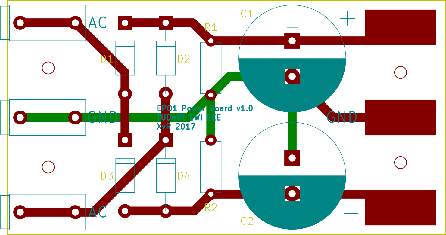
Figure 3:The power supply pcb.
Perform the following measurements:
Compare simulation with reality. Do the measured waveforms match your expectations?
Load the positive and negative outputs equally so that about 1.0 A flows. Compare measured voltage, current, and ripple with the simulation.
Determine the equivalent load resistance for which the supply output equals 19 V DC. Verify against simulation.